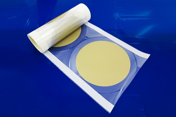
Die-Attach Film Adhesives
Die-Attach Film Adhesives
Description

Die-attach film adhesive is a type of adhesive material that is used in the assembly of semiconductor devices. It is a thin, flexible film that is placed between the die and the substrate, and then the assembly is heated to cure the adhesive and create a strong bond between the two.
Die-attach film adhesive is typically made from a mixture of polymer resins and curing agents, and it may contain filler materials such as silica or alumina to improve its thermal and electrical properties. The film is typically applied to the substrate using automated equipment, such as a pick-and-place machine or a die bonder, which places the die onto the adhesive-coated substrate.
One advantage of using die-attach film adhesive is that it can be applied with high precision, allowing for tight control over the amount and distribution of the adhesive. This can help to ensure that the die is securely attached to the substrate and that any voids or gaps in the bond line are minimized. Additionally, the use of a film adhesive can simplify the assembly process by eliminating the need for dispensing equipment and reducing the risk of voids or bubbles in the adhesive layer.
Die-attach film adhesive is commonly used in a variety of semiconductor applications, including memory devices, microprocessors, and power electronics. It is chosen based on the specific requirements of the application, such as the size and weight of the die, the thermal and electrical properties required, and the bonding process used.
In summary, die-attach film adhesive is a thin, flexible film that is used to bond semiconductor dies to substrates. It is typically made from a mixture of polymer resins and curing agents, and may contain filler materials to improve its thermal and electrical properties. Die-attach film adhesive can be applied with high precision and is commonly used in a variety of semiconductor applications.
- Die Attach Film Adhesives
- Flow-Over-Wire (FOW) Die-Attach Film Adhesive
- Dicing Tapes for Die-Attach Film Applications
| Characteristics | Electrical Resistivity (ohm-cm) | Thermal Conductivity (Watt/m-oK) | Die-shear (psi) | Tg (oC) | Film Thickness |
| -Post-curing without fixture and pressure-Meets MIL-STD-883F 5011.4-Proven reliability for multilayer stack | >1x10¹⁴ | >0.8 | >4,000 | 175 | 10 µ20 µ40 µ |
| -Curing without fixture and pressure-Meets MIL-STD-883F 5011.4-Low thermal resistance + high moisture resistance | >1x10¹⁴ | >1.8 | >2,000 | 175 | 20 µ40 µ |
| -Curing without fixture and pressure-Low thermal resistance + high moisture resistance-Meets MIL-STD-883F 5011.4 | <4x10⁻⁴ | >8.0 | >3,000 | 175 | 20 µ40 µ |
| -Optimizing flexibility and strength-Proven for extreme large devices-Meets MIL-STD-883F 5011.4-Low thermal resistance + high moisture resistance | <4x10⁻⁴ | >8.0 | >2,000 | 90/-50 | 20 µ40 µ |
| Characteristics | Electrical Resistivity (ohm-cm) | Thermal Conductivity (Watt/m-oK) | Die-shear (psi) | Tg (oC) |
Wafer level pre-lamination @70-80°C Wafer level packaging for up to 450mm Melt-flow for bonding @90-150°C Outstanding stress absorption and moisture barrier | >1x10¹⁴ | 0.2 (Unfilled) | >5,000 | 175 |
Wafer level pre-lamination @70-90°C Wafer level packaging for up to 450mm Melt-flow for bonding @100-150°C Outstanding moisture barrier | >1x10¹⁴ | 1.2 (Filled) | >5,000 | 175 |
| Characteristics | Electrical Resistivity (ohm-cm) | Peel Strength (gm-per-inch) | Film Thickness |
| UV and/or heat releasing | 1x10¹⁴ | 100/10(Post UV) | PO Base=75µ PSA= 10-15µ |
| Controlled and stable peel strength over time | 1x10¹⁴ | 100 | PO Base=75µ PSA= 10-15µ |
Controlled and stable peel strength over time Withstand minutes of exposure up to 250°C Available in anti-static version | 1x10¹⁴ 1x10⁵-9 | 100 | AIT Proprietary Base=75µ PSA= 10-15µ |
Order Form
About Semiconductor Electronics
SEMI EL project is a global supplier of materials, equipment, spare parts and supplies for the semiconductor industry.
Get In Touch
Email: info@semi-el.com

