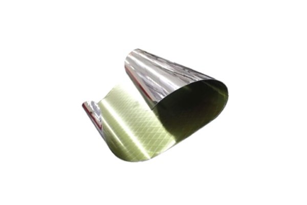
WAFER BACKGRINDING AND DICING TAPES
Wafer Backgrinding and Dicing Tapes
Description

Wafer backgrinding and dicing tapes are specialized materials used in the semiconductor industry during the process of thinning and separating wafers into individual die.
Wafer backgrinding is the process of thinning the wafer by grinding away a portion of the substrate from the backside of the wafer to reduce the thickness of the die. Dicing is the process of cutting the wafer into individual die after the backgrinding process is complete.
During these processes, a specialized tape is used to attach the wafer to a carrier substrate, which helps to prevent damage to the die and provide support during grinding and cutting. The tape also acts as a temporary adhesive, holding the thinned wafer in place during subsequent manufacturing steps.
The tape used for backgrinding and dicing is typically made of a polymer material such as polyethylene terephthalate (PET) or polyvinyl chloride (PVC), and is coated with a pressure-sensitive adhesive on one or both sides. The adhesive used on the tape is specifically designed to maintain adhesion strength even at high temperatures and after exposure to chemicals commonly used in semiconductor processing.
The selection of the appropriate backgrinding and dicing tape is dependent on various factors such as the thickness and material of the wafer, the equipment used for the process, and the specific manufacturing requirements. Manufacturers offer a wide range of tapes with different thicknesses, adhesive strengths, and release properties to suit different applications.
Overall, wafer backgrinding and dicing tapes play a critical role in the semiconductor manufacturing process, providing support and protection to delicate semiconductor wafers during thinning and cutting operations.
| PARAMETER | BG-UVR100-PET | BG-HTCR100-PET | BG-HR200-PET |
| Release Mechanism-Material and Thickness | UV Exposed | Controlled Peel | Heat Curing Release |
| Carrier Support Film and Thickness | PET or LCP 75 Microns | PET or LCP 75 microns | PET or LCP 75 microns |
| Thickness of Compressible-Compliant Layer | 150 micron version 300 micron version | 150 micron version 300 micron version | 150 micron version 300 micron version |
| Peel Strength in Operation (gpi) | 100 gpi 250gpi, 500 gpi (option) | 100 gpi 250 gpi, 500 gpi (option) | 200 gpi 100 gpi, 500 gpi (option) |
| Peel Strength for Release (gpi) | 25 gpi nominal | 100 gpi nominal | 25 gpi nominal |
| Operational Temperature Capability | 150°C (PET Version) 250°C (LCP Version) | 150°C (PET Version) 250°C (LCP Version) | Peel lower when exposed to 150°C |
| Chemical Resistance | Outstanding | Outstanding | Outstanding |
| Water Jet Resistance | Outstanding | Outstanding | Outstanding |
| Note #1: All backgrinding and thinning temporary materials are free of silicones or siloxanes. | |||
| Note #2: Anti-static versions are available for all UV, heat or peel release temporary bonding. | |||
| Product | Adhesion Before UV Exposure (Peel, gm/in) | Adhesion After UV Exposure (Peel, gm/in) | Adhesive/Buffer Thickness (Micron) | Backing Material Thickness (Micron) | Compressibility [ ] | Tensile Strength (Kg/cm) | Special Characteristics |
|---|---|---|---|---|---|---|---|
| BG-FC-UVR500 | 500 | 20 | 150 | 125 | [>100 micron] | >200 | Withstand 100°C continuous usage Silicone-Free |
| BG-SB-UVR500 | 500 | 20 | 300 | 125 | [>250 micron] | >200 | Withstand 100°C continuous usage Silicone-Free |
| Product | Push-Off Strength (Die-Shear, psi) | Max. Load Bearing Temp. (°C) | “Melt-Bonding” Temperature & Lamination Process (@14-15psi) |
|---|---|---|---|
| CB7060 (Single ply melt-bonding adhesive film) | >1,000 | 60 | >70°C with heated roll laminator with proper “foam” support >70°C with “vacuum bagging” Low ionic and ease of total removal |
| CB7130 (Single ply melt-bonding adhesive film) | >1,000 | 130 | >130°C with heated roll laminator with proper “foam” support >130°C with “vacuum bagging” Low ionic and ease of total removal |
| CB7350-S (High-tack single-sided adhesive film on a temperature stable liner) | >300 | 150 (Continuous & 300 @5 min.) | Mount wafer-substrate with suitable laminator or with “vacuum bagging” equipment Low ionic and ease of total removal with suitable solvent |
| CB7350-B (High-tack double-sided adhesive film on a temperature stable liner) | >300 | 150 (Continuous & 300 @5 min.) | Mount wafer-substrate with suitable laminator or with “vacuum bagging” equipment Low ionic and ease of total removal with suitable solvent |
| CB7065 (Thermally conductive, single ply melt-bonding adhesive film) | >1,000 | 60 | >70°C with heated roll laminator with proper “foam” support >70°C with “vacuum bagging” Low ionic and ease of total removal |
| CB7135 (Thermally conductive, single ply melt-bonding adhesive film) | >1,000 | 130 | >130°C with heated roll laminator with proper “foam” support >130°C with “vacuum bagging” Low ionic and ease of total removal |
| TK7355-SS (High-tack single-sided adhesive film on a high thermal conductivity film liner) | >300 | 150 (Continuous & 300 @5 min.) | Mount wafer-substrate with suitable laminator or with “vacuum bagging” equipment Low ionic and ease of total removal with suitable solvent |
Order Form
About Semiconductor Electronics
SEMI EL project is a global supplier of materials, equipment, spare parts and supplies for the semiconductor industry.
Get In Touch
Email: info@semi-el.com

