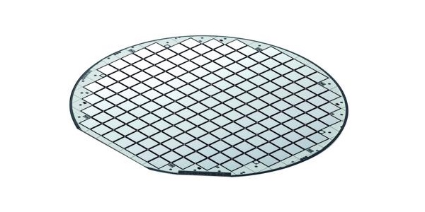
Superluminescent Diode (SLED) Chips
Superluminescent Diode (SLED) Chips
Description

Superluminescent LEDs or SLED chips come in 650nm to 1280nm range and in variety of power options. They are applied in optical measurement devices and medical imaging instruments, optical coherence tomography, interferometry, optical sensing and fiberoptic gyroscopes.
Superluminescent Diode (SLD) Chips are a type of semiconductor device that combines the emission characteristics of a laser diode and a light-emitting diode (LED). SLDs are designed to emit broad-spectrum light with high power and low coherence, making them suitable for a range of applications in optical sensing and imaging.
The operation of SLD chips is based on the same principle as laser diodes, where light is emitted through the stimulated emission process. However, in SLDs, the optical cavity is intentionally made to be much shorter than in laser diodes, resulting in a much broader spectral linewidth and lower coherence. The broad spectral output is achieved through a combination of optical gain and amplified spontaneous emission (ASE) in the active region of the device.
The active region of an SLD chip typically consists of a multi-quantum well structure, where several thin layers of different semiconducting materials are stacked on top of each other. The width of each layer is chosen to create a narrow bandgap, which allows for efficient light emission. The SLD chip is usually operated in a forward-biased configuration, where electrical current is injected into the active region to excite the electrons and generate light.
SLD chips have several advantages over traditional LEDs and laser diodes, including broad spectral output, high output power, low coherence, and low cost. They are used in a wide range of applications, including optical coherence tomography (OCT), fiber optic gyroscopes, and optical sensing and imaging.
The fabrication process for SLD chips is similar to that of laser diodes and LEDs, with additional steps to optimize the cavity length and spectral output. The process typically involves epitaxial growth of the active region and cladding layers, followed by lithography and etching to define the device structure.
| Wavelength | Bandwidth | Output power |
|---|---|---|
| 1000nm | 100 | 25 |
| 1030nm | 120 | 15 |
| 1030nm | 20 | 130 |
| 1050nm | 90 | 35 |
| 1065nm | 25 | 130 |
| 1060nm | 20 | 300 |
| 1064nm | 20 | 350 |
| 1080nm | 30 | 100 |
| 1130nm | 27 | 30 |
| 1140nm | 85 | 1 |
| 1190nm | 90 | 1 |
| 1250nm | 110 | 5 |
| 1280nm | 50 | 1 |
| 650nm | 7.5 | up to 5.0 |
| 670nm | 7.0 | up to 15.0 |
| 795nm | 15 | 20 |
| 825nm | 20 | 5 |
| 835nm | 17 | 20 |
| 850nm | 20 | 30 |
| 840nm | 25 - 30 | up to 100 |
| 880nm | 40 | 20 |
| 920nm | 30 | 20 |
| 960nm | 45 | 90 |
| 1040nm | 35 - 45 | up to 80.0 |
Order Form
About Semiconductor Electronics
SEMI EL project is a global supplier of materials, equipment, spare parts and supplies for the semiconductor industry.
Get In Touch
Email: info@semi-el.com

