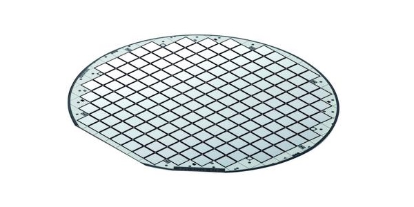
Silicon Submounts
Description

Silicon submounts are a type of package used for mounting and protecting semiconductor devices, such as photodiodes, lasers, and light-emitting diodes (LEDs). The submount acts as a platform for the device, providing mechanical support and electrical connections while also helping to dissipate heat generated by the device.
Silicon submounts are made from silicon wafers, which are highly conductive and offer good thermal conductivity. They are typically manufactured using semiconductor processing techniques, such as photolithography and etching. The submounts can be customized to fit a specific device or application, with features such as electrical contacts, alignment marks, and optical windows.
Silicon submounts are commonly used in high-speed communication systems, where they can be used to mount and protect laser diodes and photodiodes. The submounts help to improve the performance of these devices by reducing thermal noise and ensuring proper alignment with other optical components.
One advantage of using silicon submounts is their compatibility with semiconductor processing techniques. This allows for integration with other semiconductor devices, such as microprocessors and memory chips, in a single package. Additionally, the high thermal conductivity of silicon allows for efficient heat dissipation, which can help to extend the lifetime of the device.
Chip size - 10*10 mil
Order Form
About Semiconductor Electronics
SEMI EL project is a global supplier of materials, equipment, spare parts and supplies for the semiconductor industry.
Get In Touch
Email: info@semi-el.com

