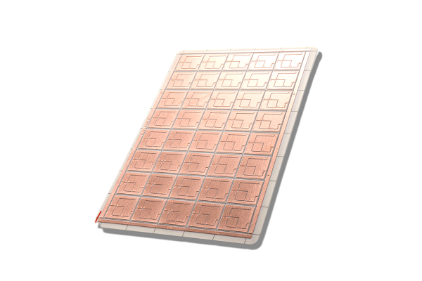
Active Metal Brazing (AMB) Technology Ceramic Substrates
Active Metal Brazing (AMB) Technology Ceramic Substrates
Description

Active Metal Brazing (AMB) technology ceramic substrates are a type of substrate used in electronic devices that require high thermal conductivity and good mechanical stability. AMB technology involves joining ceramic substrates to metal layers using a specialized brazing process.
The brazing process involves applying a thin layer of a specialized active metal alloy to the ceramic substrate surface, which is then heated to a high temperature in the presence of a reducing gas atmosphere. This causes the active metal to react with the ceramic and form a strong chemical bond, allowing the metal layer to be joined to the ceramic substrate.
AMB technology substrates are commonly used in high-power electronic applications, such as power modules for electric vehicles and renewable energy systems, where the ability to dissipate heat quickly is essential for device performance and reliability. The use of AMB technology allows for the creation of high-performance power modules with improved thermal management and reduced size, weight, and cost compared to traditional wire-bonded packages.
AMB or Active Metal Brazing is the most promising thick film technology and the main competing technology is DBC. In AMB ceramic substrate technology there was found a solution of discrepancy between thermal expansion coefficients of copper and ceramic substrate by introducing buffer layer between conductor and ceramic substrate. This buffer layer releases strain between the layers during thermal cycling and also serves as the adhesion layer.
The buffer layer can be deposited by CVD or PVD technology as well as with special solder pastes. The main thickness of copper is grown by galvanic method. The weak point of the Active Metal Brazing technology is thermal conductivity of buffer layer that reduces the thermal conductivity of conducting layer therefore AlN substrates are recommended to be used in this technology. AMB ceramic PCBs are a good choice for high-temperature H2 soldering. The PCBs have extreme thermal and energy cycle resistivity (more than 15000 energy cycles on/off at 100C and more than 5000 cycles in 200C.)
| Method characteristics | ||||
| Bubbles in the solder joint | <5% of the total junction area (1 bladder area <1%) | |||
| Conductive layer thickness *, microns | from 100 to 800 | |||
| Ceramic used | AlN, Al 2 O 3 | |||
| Peel strength of copper, N / mm 2 | > 15 | |||
* The maximum conductive layer thickness is determined by the type and thickness of the ceramic substrate.
| Copper thickness | Method resolution | |||
| Distance between conductors, mm | Conductor width, mm | |||
| A type. | Min. | A type. | Min. | |
| 0.127 | 0.30 | 0.25 | 0.30 | 0.25 |
| 0.20 | 0.50 | 0.40 | 0.50 | 0.40 |
| 0.25 | 0.60 | 0.50 | 0.60 | 0.50 |
| 0.30 | 0.70 | 0.50 | 0.70 | 0.50 |
| 0.40 | 0.80 | 0.60 | 0.80 | 0.60 |
Order Form
About Semiconductor Electronics
SEMI EL project is a global supplier of materials, equipment, spare parts and supplies for the semiconductor industry.
Get In Touch
Email: info@semi-el.com

