Direct Bonded Copper (DBC) Technology Substrates
Direct Bonded Copper (DBC) Technology Substrates
Description

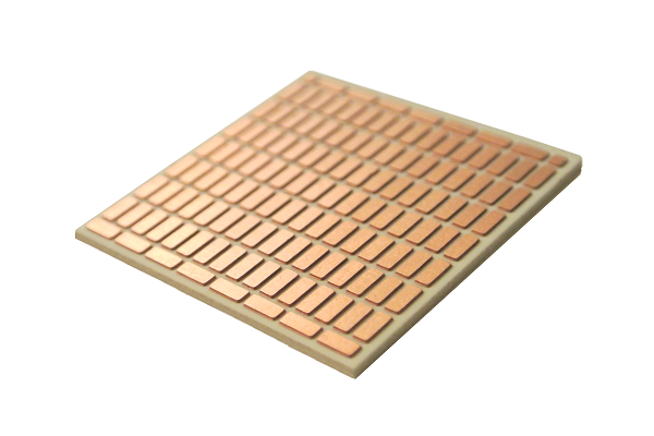
Direct Bonded Copper (DBC) technology substrates are a type of substrate used in electronic devices that require high thermal conductivity and good electrical insulation. DBC substrates consist of a ceramic substrate, such as aluminum nitride or alumina, that is bonded directly to a copper layer using a high-temperature bonding process.
The ceramic substrate provides good electrical insulation and mechanical stability, while the copper layer provides high thermal conductivity and good electrical conductivity. The copper layer is typically patterned to form circuit traces and pads using a photoresist and etching process.
DBC technology substrates are commonly used in high-power electronic applications, such as power modules for electric vehicles and renewable energy systems, where the ability to dissipate heat quickly is essential for device performance and reliability. The use of DBC substrates allows for the creation of high-performance power modules with reduced size, weight, and cost compared to traditional wire-bonded packages.
DBC or Direct Bonded Copper technology, sometimes called DCB (Direct Copper Bonding), is the most efficient technology for bonding copper foil with 120 to 700um thickness to AlN or Al2O3 ceramic substrate. This technology has a wide application sphere such as:
- Thermoelectric and Peltier modules
- Power integrated circuits
- RF devices
- Powertrain engines
- Medical equipment
- Semiconductor devices
- Automotive electronics
DBC technology allows to create ceramic PCBs with a topology similar to PCB etching technology, at the same time thick copper conductors provide good conductivity and thermal sinking from semiconductor chips. This technology allows soldering in a wide temperature range from 180 to 850C, low thermal expansion coefficient that keeps stable characteristics of the device in thermal cycling up to 50000 cycles.
DBC substrates can work in -100 to 250C and can withstand higher currents up to thousands of volts compared to other metallization methods such as screen printing or electrochemical plating. Also this technology allows to produce ceramic PCBs with vias.
| Characteristic | Meaning |
| Basic substance content,% | 99,00 |
| Static bending strength, MPa | 193.90 |
| Specific volumetric electrical resistance (at 25 о С), Ohm • cm | 40.00 ∙ 10 14 |
| Loss tangent (frequency range 8-10 GHz) | 1.50 ∙ 10 -4 |
| Dielectric constant (frequency range 8-10 GHz) | 7.30 |
| TCLE ( ∙ 10 -7 1 / о С) in the temperature range, о С | |
| 20 - 200 | 59.00 |
| 20 - 500 | 70,00 |
| 20 - 900 | 77,00 |
| 20 - 1000 | 80,00 |
| Porosity,% | 0.07 |
| Thermal conductivity (at 20 о С), W / m ∙ deg | 21.00 |
| Equivalent thermal conductivity, W / m ∙ deg | 209.50 |
| Breakdown voltage, kV | 15.00 |
Characteristics of conductive tracks
| Copper thickness, mm | Distance between conductors, mm | Conductor width, mm | ||
| A type. | Min. | A type. | Min | |
| 0.127 | 0.30 | 0.25 | 0.30 | 0.25 |
| 0.20 | 0.50 | 0.40 | 0.50 | 0.40 |
| 0.25 | 0.60 | 0.50 | 0.60 | 0.50 |
| 0.30 | 0.70 | 0.50 | 0.70 | 0.50 |
| 0.40 | 0.80 | 0.60 | 0.80 | 0.60 |
| 0.50 | 0.90 | 0.70 | 0.90 | 0.70 |
Types of ceramics used
| Parameter | Meaning |
| Backing material | Al 2 O 3 (96%), AlN |
| Maximum substrate size, mm | 138 x 188 |
| Substrate thickness, mm | 0.25; 0.38; 0.5; 0.635; 0.76; one |
| Loss tangent (250 o С / 1 MHz) | ≤ 3 ∙ 10 -4 |
| Thermal conductivity W / (m ∙ K) | > 24 |
| Dielectric strength | > 14 |
| Dielectric constant (250 o С / 1 MHz) | ≤ 9.4 |
Copper plating characteristics
| Parameter | Meaning |
| Thermal conductivity W / (m • K) | 385 |
| Thickness, mm | 0.07 - 0.4 ... 0.3 ± 0.015 |
| Chemical composition, % | 99.99 |
| Breakout force, N / mm | >6 |
| Working temperature, ℃ | from -55 to +850 |
| Surface roughness Ra, μm | ≤ 3 |
| Etching defects, μm | ≤ 30 |
Possible topcoats
| Abbreviation | Layer thickness |
| HASL (Hot Air Solder Leveling) | from 15 to 25 microns |
| HAL (Hot Air Leveling) Lead free (Pb free) | from 15 to 25 microns |
| ENIG (Electroless Nickel / Immersion Gold) | Ni from 3 to 8 microns, Au 0.08 to 0.15 |
| Flash Gold | Ni from 3 to 8 microns, Au from 0.08 to 0.15 μm |
| Immersion Tin | from 0.8 to 1.2 μm |
| Immersion silver | from 0.05 to 0.20 μm |
| OSP (Organic Solderability Preservative) Entek plus | 0.2 to 0.6 μm |
| Soft gold | Ni from 3 to 8 microns, Au 0.2 to 0.5 μm |
| HARD GOLD for Edge Connectors | Ni from 3 to 8 microns, Au 1.5 to 3 μm |
Order Form
About Semiconductor Electronics
SEMI EL project is a global supplier of materials, equipment, spare parts and supplies for the semiconductor industry.
Get In Touch
Email: info@semi-el.com

