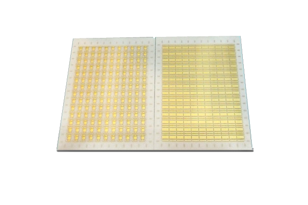
Direct Plated Copper (DPC) Technology Substrates
Direct Plated Copper (DPC) Technology Substrates

Description
DPC substrates have a wide range of applications such as:
- Solar collectors;
- Power electronics, power integrated circuits;
- Thermoelectric coolers and generators;
- Mmicrowave and RF devices;
- LEDs
Due to high-resolution DPC technology allows to achieve higher density of packaging. Topology resolution is defined by the thickness of copper metallization necessary. The ratio of thickness and thickness of conductor is 3:1, thus at 20um thickness the width of conductor can be as small as 60um.
Unlike thick film technology DPC films do not have a glass phase therefore having higher thermal and electrical conductivity. This makes them a proper material in power electronics. DPC films have high metal purity, low roughness and excellent adhesion. DPC technology is the lowest cost and highest throughput technology among all thick film and thin-film metallization technologies. AlN and Al2O3 ceramics are used as substrate materials for this technology.
Unlike thick copper conductive films, films formed by the DPC method do not have a glass phase in their structure, due to which they have higher electrical and thermal conductivity. This makes them very promising for applications in power electronics.
Films formed using DPC technology have extremely high material purity, low surface roughness and excellent adhesion properties.
Comparison of topology made with DPC technology and thick film technology
| Name | Thick film technology | DPC technology |
| Topology fabrication accuracy | ± 10% | ± 1% |
| Adhesion | low | high |
| Roughness, μm | from 1 to 3 | ≤ 0.3 |
| Topology image |  |  |
Among the classic thin-film and thick-film methods, DPC technology is the cheapest and most productive, while having the best physical and mechanical properties.
Comparison of technologies on a 5-point scale (5 is the best indicator, 1 is the worst indicator)
| Parameter | DPC technology | Thin film technology | Thick film technology |
| Electrical conductivity | five | 3 | 4 |
| Thermal conductivity | five | 3 | 4 |
| Stability of parameters | five | five | 3 |
| Resolution | 4..5 (determined by the thickness of the copper layer) | five | 2 |
| Price | five | 2 | 2 |
AlN and Al2O3 ceramics are used as substrates. The thickness of the copper conductive layer is determined by the customer.
| Ceramic material | Metallization material / thickness, microns | Vias conductive material | Conductor width tolerance, microns | ||
| Copper (Cu) | Nickel (Ni) | Gold (Au) | |||
| Al2O3 | 1 to 100 | 3 to 5 | 0.075 to 1 | Silver, copper, silver / copper | fifty |
| AlN | |||||
An equally important characteristic that determines the durability of products is the resistance of the metallized board to temperature effects. Thermal cycling testing was conducted per MIL-STD-202.107G. This method is designed to determine the resistance of a metalized ceramic substrate to temperature cycling.
Test conditions:
• -400C (30 min) ~ 1250 o C (30 min), 500 cycles;
• adhesion measurement method: tensile testing machine;
• conditions: adhesion ≥ 3 kg.
Test results
| No. | Value, kg | Result | No. | Value, kg | Result |
| one | 3.84 | + | 6 | 3.94 | + |
| 2 | 3.92 | + | 7 | 4.11 | + |
| 3 | 4.02 | + | eight | 3.51 | + |
| 4 | 3.76 | + | nine | 3.87 | + |
| five | 3.58 | + | 10 | 4.01 | + |
| Average value of adhesion, kg: 3.86 ± 0.18 | |||||
Order Form
About Semiconductor Electronics
SEMI EL project is a global supplier of materials, equipment, spare parts and supplies for the semiconductor industry.
Get In Touch
Email: info@semi-el.com

