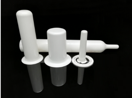
Pyrolytic Boron Nitride
Pyrolytic Boron Nitride
Description

Pyrolytic boron nitride (PBN) is a high-purity ceramic material that is commonly used in high-temperature applications, such as in semiconductor manufacturing and high-temperature furnace components. It is made by the chemical vapor deposition of boron nitride onto a substrate, typically a graphite material.
PBN has a unique layered structure, similar to that of graphite, but with boron and nitrogen atoms arranged in a hexagonal lattice. This gives it excellent thermal and electrical properties, such as high thermal conductivity, high electrical resistivity, and low dielectric loss at high frequencies.
PBN is often used as a coating or as a substrate material for high-temperature applications where other materials would degrade or fail, such as in the production of silicon wafers or in the growth of compound semiconductors like gallium nitride. It is also used as a crucible material for the growth of single crystals of high-melting-point metals and compounds.
PBN has several advantages over other high-temperature materials like ceramics or metals. It has a very low coefficient of thermal expansion, which means that it will not expand or contract significantly with changes in temperature. It is also resistant to chemical attack from many acids, bases, and organic solvents.
Pyrolytic Boron Nitride is an advanced ceramic material, produced by CVD process. Compared with normal boron nitride material, PBN has much better purity level and advantages. It is an ideal material for crystal growing and high vacuum processes. PBN can be easily machined into shapes for use as crucibles, boats, plates, tubes and bottles, and other applications.
Advantages:
● Non-toxic.
● Non-wetting
● High purity(>99.99%).
● High thermal conductivity.
● High electrical resistance.
● Excellent thermal shock resistance.
● High working temperature (>2000°C).
● Non-reactive to most other compounds.
Applications:
● OLED Production
● MOCVD Heater
● Polycrystalline Synthesis
● Molecular Beam Epitaxy (MBE)
● Compound Semiconductor Crystal Growth
● Satellite Communication TWT
| Item | Unit | Value | ||
| Density | g/cm3 | 1.95-2.20 | ||
| Lattice Constant | μm | a: 2.504×10⁻¹⁰ c: 6.692×10⁻¹⁰ | ||
| Volume Resistivity | Ω·cm | 3.11×10¹¹ | ||
| Tensile Strength (ab) | N/mm2 | 153.86 | ||
| Bending Strength | c | N/mm2 | 243.63 | |
| ab | N/mm2 | 197.76 | ||
| Elastic Modulus | N/mm2 | 235690 | ||
| Thermal Conductivity | 200℃ | W/m·k | a: 60 | c: 2.6 |
| 900℃ | W/m·k | a: 43.7 | c: 2.8 | |
| Dielectric Strength (at room temperature) | KV/mm | 56 | ||
Order Form
About Semiconductor Electronics
SEMI EL project is a global supplier of materials, equipment, spare parts and supplies for the semiconductor industry.
Get In Touch
Email: info@semi-el.com

