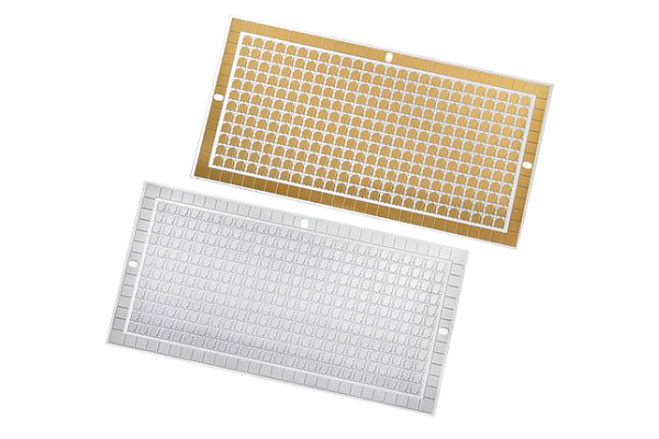
Thin-Film Technology Substrates
Thin-Film Technology Substrates
Description

Thin-film technology substrates are a type of substrate used in electronic devices that rely on thin layers of materials to create circuits and components. Thin-film technology involves depositing a thin layer of a conductive, insulating, or semiconducting material onto a substrate using a variety of deposition techniques, such as sputtering, chemical vapor deposition (CVD), and physical vapor deposition (PVD).
Thin-film technology substrates are typically made of materials such as glass, quartz, silicon, or ceramics. These materials offer good mechanical stability, thermal conductivity, and chemical resistance, which are essential for the thin-film deposition process and the resulting electronic devices.
Thin-film technology substrates are commonly used in a variety of electronic applications, including flat panel displays, solar cells, optical coatings, and microelectronics. In these applications, the thin-film layers are used to create circuits, transistors, diodes, capacitors, resistors, and other components. The use of thin-film technology allows for precise control over the properties of the material layers, such as their thickness, composition, and electrical properties, resulting in high-performance electronic devices with improved functionality and reliability.
In thin-film technology adhesive and base functional layers are deposited onto ceramic substrate. The deposition is done by PVD, CVD or ALD methods. PVD methods are easy and productive methods, therefore prequesntly used in this technology. ALD and CVD methods have a major disadvantage- low deposition rate. In case the thickness of the deposited layer is not sufficient extra thickness is grown galvanically. For topology of PCB forming lithography process is used.
Thin-film substrates have embedded active and passive elements that allow to decrease dimensions and increase speed. The base material for thin-film technology is AlN and Al2O3, copper and aluminum are used for conductive layers. Optically transparent ITO films can be formed on thin-film substrates.
Specification of products sold using thin-film technology, check with our specialists.
Order Form
About Semiconductor Electronics
SEMI EL project is a global supplier of materials, equipment, spare parts and supplies for the semiconductor industry.
Get In Touch
Email: info@semi-el.com

