Diamond on GaN Wafers
Diamond on GaN Wafers
Description

Diamond on GaN wafers are a type of heterostructure material composed of a thin diamond layer deposited on a gallium nitride (GaN) substrate. The diamond layer is typically grown using chemical vapor deposition (CVD) techniques, which allows for precise control over the diamond layer thickness and quality.
Diamond on GaN wafers have unique electronic and thermal properties that make them suitable for various applications, such as high-power electronic devices, high-frequency transistors, and high-temperature sensors. The combination of diamond's high thermal conductivity and GaN's high electron mobility can result in devices that exhibit both high power and high efficiency.
One of the primary advantages of diamond on GaN wafers is their high thermal conductivity, which allows them to dissipate heat more efficiently than traditional materials such as silicon or GaN. This property makes diamond on GaN wafers ideal for use in high-power devices such as RF power amplifiers and power electronics.
Diamond on GaN wafers also have a wide bandgap, which allows them to operate at high temperatures without degradation. This makes them suitable for use in high-temperature sensors and electronic devices that need to operate in harsh environments.
Diamond on GaN wafers are an exciting area of research in the field of materials science and have the potential to enable the development of advanced electronic and optoelectronic devices with high performance and efficiency.
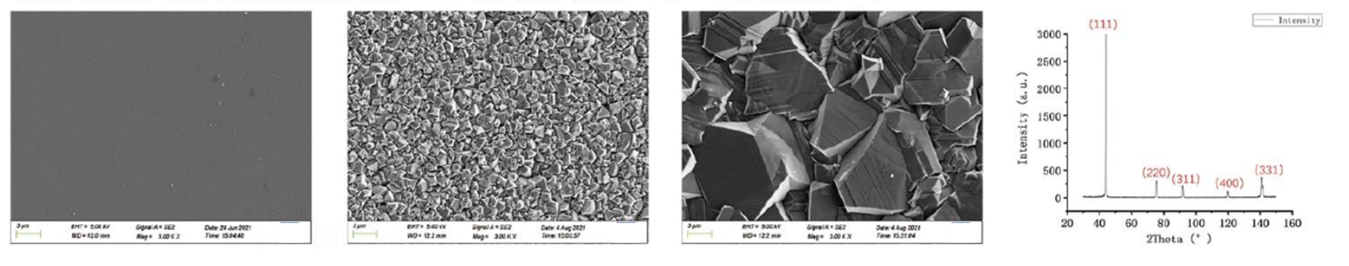
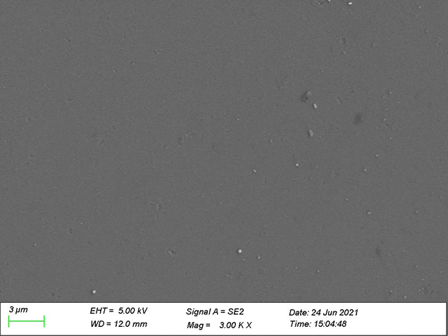
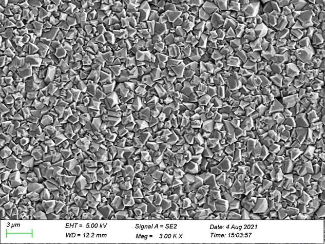
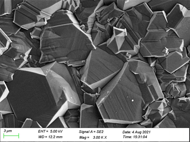
We uses microwave plasma chemical vapor deposition (MW CVD) equipment to epitaxially grow polycrystalline diamond layer <10um on a 50.8 mm (2 inch) GaN-on-Si HEMT. SEM and X-ray diffractometer characterization of the surface morphology, crystalline quality, and grain orientation of the diamond film were performed. The results showed that the surface morphology of the sample was relatively uniform, and the diamond grains basically showed a (111) plane growth. During the growth process, the gallium nitride (GaN) was prevented from hydrogen plasma etching, therefor the characteristics of the GaN layer before and after the diamond coating were not significantly affected.
Order Form
About Semiconductor Electronics
SEMI EL project is a global supplier of materials, equipment, spare parts and supplies for the semiconductor industry.
Get In Touch
Email: info@semi-el.com