GaN / Diamond Bonded Wafer
GaN / Diamond Bonded Wafer
Description

GaN/diamond bonded wafers are a type of hybrid wafer that combines the properties of gallium nitride (GaN) and diamond materials. The wafer consists of a thin layer of GaN deposited on a diamond substrate using various deposition techniques such as metalorganic chemical vapor deposition (MOCVD) or molecular beam epitaxy (MBE). The GaN layer can be either n-type or p-type depending on the doping type used during the growth process.
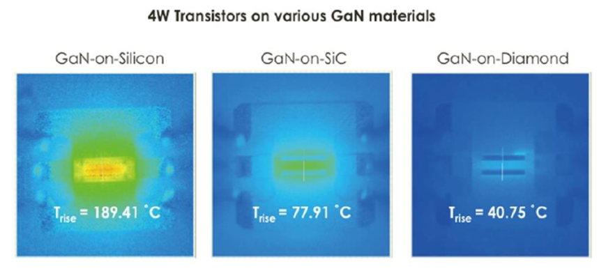
The diamond substrate offers several advantages over traditional silicon substrates used for GaN growth. The high thermal conductivity of diamond helps to dissipate the heat generated by the GaN device during operation, which can improve the reliability and lifetime of the device. Diamond also has a high breakdown field strength, making it ideal for high-power and high-frequency applications.
The GaN layer on the diamond substrate can be used to fabricate various electronic and optoelectronic devices such as high-electron mobility transistors (HEMTs), metal-insulator-semiconductor (MIS) devices, and light-emitting diodes (LEDs). The GaN/diamond wafer can also be used as a template for the growth of other III-V nitride materials such as AlGaN and InGaN.
The bonding between the GaN layer and the diamond substrate is typically achieved using a thin intermediate layer such as titanium or chromium. The bonding process can be done using various methods such as wafer bonding, surface-activated bonding, or metal-mediated bonding.
The technical parameters of our diamond heat sink and wafer form diamond substrates have become the industry standard. The surface roughness of the wafer-level diamond surface achieves Ra<1nm, and the thermal conductivity of the diamond heat sink can be up to 2000W/m.K. By bonding GaN with diamond substrate, the temperature of the device can be effectively reduced thus improving the stability and lifetime of the device.
Order Form
About Semiconductor Electronics
SEMI EL project is a global supplier of materials, equipment, spare parts and supplies for the semiconductor industry.
Get In Touch
Email: info@semi-el.com