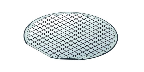
Lithium Niobate Thin Films (LNOI)
Lithium Niobate Thin Films (LNOI)
Description

Lithium niobate thin films (LNOI) are a type of optical material made of a thin layer of lithium niobate deposited on a substrate using various deposition techniques such as sputtering or pulsed laser deposition. LNOI is a ferroelectric material that exhibits spontaneous polarization, making it useful in various applications such as optical modulators, filters, and switches.
One of the key advantages of LNOI is its high electro-optic coefficient, which allows for efficient modulation of light using an electric field. This property makes LNOI ideal for use in optical modulators, where changes in the refractive index of the material can be used to modulate the intensity or phase of light in optical communication systems.
LNOI thin films also have a high refractive index, making them useful in waveguide applications such as optical interconnects, sensors, and detectors. The high refractive index allows LNOI to confine and guide light, which can be used to create optical circuits that perform various functions.
Another advantage of LNOI thin films is their piezoelectric properties, which allow them to convert mechanical energy into electrical energy and vice versa. This property can be utilized in various applications such as sensors and energy harvesting devices.
LNOI thin films are a critical component in the development of advanced optical devices and systems. Their unique optical, electrical, and mechanical properties make them ideal for use in various applications, from telecommunications to biophotonics.
| 300-900 nm Lithium Niobate Thin Films (LNOI) | ||||
| Top Functional Layer | ||||
| Diameter | 3, 4, (6) inch | Orientation | X, Z, Y etc. | |
| Material | LiNbO3 | Thickness | 300-900 nm | |
| Doped (optional) | MgO | |||
| Isolation Layer | ||||
| Material | SiO2 | Thickness | 1000-4000 nm | |
| Substrate | ||||
| Material | Si, LN, Quartz, Fused Silica etc. | |||
| Thickness | 400-500 μm | |||
| Optional Electrode Layer | ||||
| Material | Pt, Au, Cr | Thickness | 100-400 nm | |
| Structure | Above or Under SiO2 Isolation Layer | |||
| 5-50 μm LN on Si | ||||
| Top Functional Layer | ||||
| Diameter | 3, 4, 6 inch | Orientation | X, Z, Y-42, Y-46.3 etc. | |
| Material | LiNbO3 etc. | Thickness | 5-50 μm | |
| Substrate | ||||
| Material | Si | |||
| Thickness | 230-500 μm | |||
| Free Standing Ultra Thin & Ultra Flat Wafers | |||
| Diameter | 3, 4 inch | Orientation | X, Y, Z etc. |
| Thickness | 10-60 um | Material | LN |
| Surface | Double or Single Side Polished | ||
| Customized Lithium Niobate Thin Films | ||||||||
| Top Layer/ Details | Substrate Details | Top Layer Thin Films Details | ||||||
| Multi Layer Structure | Patterned Electrode & Waveguide | Different Material (SiO2/Si, Si, Sapphire, Quartz etc.) | PPLN | Special Size | Electrode (Au, Pt, Cr, Al etc.) | Orientation (Same as Bulk Wafers ) | Doped (MgO, Fe, Er, Tm etc.) | |
| 100-1000 nm LiNbO3 | √ | √ | √ | √ | √ | √ | √ | √ |
| 5-50 um LiNbO3 | √ | √ | √ | √ | ||||
FAQ
Question 1:
I need LNOI wafer with the following specs: 50 nm Pure Si / 300 nm LN x-cut/ ~ 5 µm SiO2/ 500 µm Si (100) (any doping).
Question 2:
I need a wafer consisting of the following layers:
- 30nm crystalline - Si
- 300 nm LiNbO3 (or 300 nm Si3N4)
- 2 µm SiO2
- ~ 500 µm
The problem is crystalline Si on top, which I assume is not possible to make by deposition and all deposition methods create amorphous Si (Correct me if I am wrong). Can you produce such a wafer or a similar wafer?
Answer:
The structure we can do: Si/SiO2 layer/x-cut LN thin film/Thermal Oxide/Si handle wafer, please refer to the sturcture and let me know the thickness of every layer you prefer. For the LNOI, we recommend x-cut, 360nm or 600nm LN/4.7um Thermal Oxide/Si, these two are our mass produced LNOIs, which cost would be lower than others. So the answer to you question is yes, provided we add oxide layer between LN and Si
Order Form
About Semiconductor Electronics
SEMI EL project is a global supplier of materials, equipment, spare parts and supplies for the semiconductor industry.
Get In Touch
Email: info@semi-el.com

