Lithium Tantalate Thin Films (LTOI)
Lithium Tantalate Thin Films (LTOI)
Description

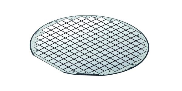
Lithium Tantalate thin films grown on silicon belong to the category of piezoelectric on insulator engineered semiconductor substrates. The standard substate is high resisitivity silicon, apop of that layer a layer of silicon oxide SiO2 is grown, and next LN thin films are grown. The LTOI wafers are used primarily for high speed SAW filter devices and modulators for 4G and 5G networks.
Lithium Tantalate (LiTaO3) thin films are a type of ferroelectric material that has received significant attention in the field of electronics and photonics due to their excellent electrical, optical, and mechanical properties. These properties make them highly suitable for use in a wide range of applications, including waveguide devices, electro-optic modulators, frequency control devices, and micro-electromechanical systems (MEMS).
One of the primary advantages of LiTaO3 thin films is their high electromechanical coupling coefficient, which makes them highly responsive to electrical stimuli. They also have a high dielectric constant, which allows them to store a large amount of charge. This property makes them useful in the fabrication of capacitors and other electronic components.
In addition to their electrical properties, LiTaO3 thin films also have excellent optical properties. They have a high refractive index and a low optical loss, which makes them highly suitable for use in waveguide devices, such as optical filters and modulators.
The deposition of LiTaO3 thin films is typically carried out using techniques such as sputtering, pulsed laser deposition (PLD), and metalorganic chemical vapor deposition (MOCVD). These techniques allow for the precise control of film thickness and composition, which is essential for the fabrication of high-quality thin films.
| 300-900 nm Lithium Tantalate Thin Films (LTOI) | ||||
| Top Functional Layer | ||||
| Diameter | 3, 4, 6 inch | Orientation | Y-42, Y-46.3, Z etc. | |
| Material | LiTaO3 | Thickness | 300-900 nm | |
| Isolation Layer | ||||
| Material | SiO2 | Thickness | 300-4000 nm | |
| Substrate | ||||
| Material | Si | |||
| Thickness | 400-500 μm | |||
| 5-50 μm LT on Si | ||||
| Top Functional Layer | ||||
| Diameter | 3, 4, 6 inch | Orientation | X, Z, Y-42, Y-46.3 etc. | |
| Material | LiTaO3 etc. | Thickness | 5-50 μm | |
| Substrate | ||||
| Material | Si | |||
| Thickness | 230-500 μm | |||
| Free Standing Ultra Thin & Ultra Flat Wafers | |||
| Diameter | 3, 4 inch | Orientation | X, Y, Z etc. |
| Thickness | 10-60 um | Material | LT |
| Surface | Double or Single Side Polished | ||
| Customized Lithium Niobate Thin Films | |||||||
| Top Layer/ Details | Substrate Details | Top Layer Thin Films Details | |||||
| Multi Layer Structure | Patterned Electrode & Waveguide | Different Material (SiO2/Si, Si, Sapphire, Quartz etc.) | Special Size | Electrode (Au, Pt, Cr, Al etc.) | Orientation (Same as Bulk Wafers ) | Doped (MgO, Fe, Er, Tm etc.) | |
| 100-1500 nm LiTaO3 | √ | √ | √ | √ | √ | √ | √ |
| 5-50 um LiTaO3 | √ | √ | √ | √ | |||
Order Form
About Semiconductor Electronics
SEMI EL project is a global supplier of materials, equipment, spare parts and supplies for the semiconductor industry.
Get In Touch
Email: info@semi-el.com

