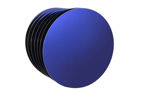
Silicon on Insulator (SOI) Wafers
Silicon on Insulator (SOI) Wafers
Description

Silicon on Insulator (SOI) wafers are a type of semiconductor substrate that consist of a thin layer of silicon (typically 50-200 nm) on top of an insulating layer, such as silicon dioxide or sapphire. The insulating layer separates the thin silicon layer from the bulk silicon substrate, which can help to reduce parasitic capacitance and improve device performance.
SOI wafers are used in various electronic applications, including microprocessors, memory devices, and radio frequency (RF) circuits. They are particularly useful in applications where high performance and low power consumption are critical, as the insulating layer can help to minimize leakage currents and reduce power consumption.
One of the key advantages of SOI wafers is their ability to reduce parasitic capacitance, which can limit the performance of advanced semiconductor devices. The insulating layer between the thin silicon layer and the bulk silicon substrate can reduce parasitic capacitance, which in turn can improve device speed and reduce power consumption.
SOI wafers also offer greater design flexibility compared to traditional bulk silicon wafers. The thin silicon layer can be patterned and processed independently of the bulk silicon substrate, which allows for greater control over device performance and functionality.
SOI wafers are an important tool for the development of advanced semiconductor devices, and play a critical role in advancing technology in fields such as computing, telecommunications, and consumer electronics.
Main applications of SOI wafers are MEMS, sensor, RF and power devices.
| Parameter | Specification Range | |
| Wafer Diameter | 100, 125, 150 mm | 200 mm |
| Handle Layer Specifications | ||
| Handle Thickness | 200–1100 µm | 450-1100 µm |
| Handle Thickness Tolerance | ±5 µm | |
| Stack Thickness | 280–1150 µm | |
| Dopant Type | N or P | |
| Doping | N type: Phos, Red Phos, Sb & As P type: Boron | |
| Resistivity | ≤0.001 – ≥10000 Ω-cm | |
| Growth Method | CZ, MCZ or FZ | |
| Crystal Orientation | <100>, <111> or <110> | |
| Backside Finish | Lapped/Etched or Polished | |
| Buried Oxide Specifications | ||
| Thermally Oxidised Buried Oxide Thickness | 0.2 – 4.0 µm grown on Handle, Device or both wafers | |
| Device Layer Specifications | ||
| Device Layer Thickness | ≥1.5 µm | ≥5 µm |
| Tolerance | ± 0.5 µm | ± 0.8 µm |
| Dopant Type | N or P | |
| Doping | N type: Phos, Red Phos, Sb & As P type: Boron | |
| Resistivity | ≤0.001 – ≥10000 Ω-cm | |
| Growth Method | CZ, MCZ or FZ | |
| Crystal Orientation | <100>, <111> or <110> | |
| Buried Layer Implant | N type or P type | |
Order Form
About Semiconductor Electronics
SEMI EL project is a global supplier of materials, equipment, spare parts and supplies for the semiconductor industry.
Get In Touch
Email: info@semi-el.com

