something else
III-V Epitaxial Wafers
Description

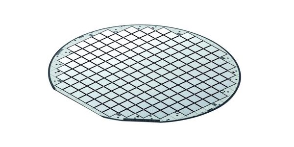
III-V epitaxial wafers are semiconductor substrates made from materials that consist of elements from the third and fifth columns of the periodic table, such as gallium arsenide (GaAs), indium phosphide (InP), and gallium nitride (GaN). The term "epitaxial" refers to the process of growing a thin layer of high-quality crystal material on top of a substrate using a technique called epitaxy.
Wafer size: 2-inch, 3-inch, 4-inch, 6-inch
Applications:
- THz, Schottky Diode, PIN detector, Laser, Photodetectors, Solar Cell;
- HEMT, mHEMT;
- LED wafer, solid state lighting;
- IR detector, PIN, sensing, IR camera;
- High speed IC/microprocessors;
One of the key advantages of III-V epitaxial wafers is their high electron mobility, which allows for faster electron transport and improved device performance compared to traditional silicon-based devices. They also have high optical gain, which makes them suitable for use in optoelectronic applications such as lasers and LEDs.
Another advantage of III-V epitaxial wafers is their ability to operate at high frequencies and high temperatures. This makes them suitable for use in high-power and high-frequency applications such as RF amplifiers and power electronics.
Rf Wafer Capability
| Product | Base Material | Material Capability | Wafer Diameter |
| HBT | GaAs | InGaP/GaAs, AlGaAs/GaAs | up to 150mm |
| InP | InP/InGaAs | up to 100mm | |
| BiFET | GaAs | InGaP/GaAs, AlGaAs/GaAs | up to 150mm |
| InP | InP/InGaAs, InP/InAlAs | up to 100mm | |
| FET | GaAs | AlGaAs/GaAs, InGaP/GaAs | up to 150mm |
| InP | InP/InGaAs, InP/InAlAs | up to 100mm |
Photonics Wafer Capability
| Product | Base Material | Material Capability | Wafer Diameter |
| Laser (VCSEL, EEL, LED) | GaAs | AlGaAs/GaAs, InGaP/GaAs, InAlGaP | up to 150mm |
| InP | InP/InGaAs, InGaAsP, InAlAs, InAlGaAs | up to 100mm | |
| Detector (P-i-N, APD) | GaAs | AlGaAs/GaAs, InGaP/GaAs | up to 150mm |
| InP | InP/InGaAs, InGaAsP, InAlGaAs | up to 100mm | |
| Solar (1J, 2J, 3J, 4J) | GaAs, Ge | InGaP/GaAs/InGaAs, InAlGaP, AlGaAs | up to 150mm |
| InP | InP/InGaAs, InGaAsP, InAlAs, InAlGaAs | up to 100mm |
Order Form
About Semiconductor Electronics
SEMI EL project is a global supplier of materials, equipment, spare parts and supplies for the semiconductor industry.
Get In Touch
Email: info@semi-el.com

