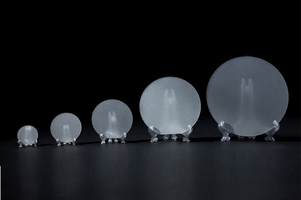
Bulk-AlN Wafers
Bulk-AlN Wafers
Description

Bulk AlN wafers are a new and very promising material with main application in UV-C LED, UV detector and laser diode chips and power and RF semiconductos. Compared to SiC and sapphire wafer templates with thin layer of GaN grown atop of these wafers, AlN substrates allow to grow better quality layers with less stress and dislocation density, thus allowing for higher device yield.
Bulk Aluminum Nitride (AlN) wafers are a type of semiconductor material used in the production of electronic and optoelectronic devices that require high thermal conductivity and high-power operation. AlN is a wide-bandgap semiconductor material, which means that it has a larger bandgap than conventional semiconductors such as silicon.
AlN wafers are typically produced using the sublimation method, which involves heating a substrate made of AlN to a high temperature in a vacuum chamber. The heat causes the AlN to sublime, or transition from a solid to a gas, and then deposit onto a cooler substrate. The deposited AlN forms a single crystal layer, which can be further processed to create wafers.
Once the AlN crystal is grown, it is sliced into thin wafers and polished to a high degree of flatness and smoothness. The resulting AlN wafers can then be used as a platform for the growth of additional semiconductor layers, which can be doped with impurities to create p-type and n-type regions for device fabrication.
AlN wafers have several advantages over other semiconductor materials such as silicon. AlN has a high thermal conductivity, which makes it suitable for high-power electronic devices that generate a lot of heat. Additionally, AlN has a wide bandgap, which makes it suitable for applications such as high-temperature electronics and deep-ultraviolet optoelectronics.
| Parameter Name | 15 mM | 50.8 mM (2") |
| Thickness, mM | 0.4 ± 0.03 | 0.4 ± 0.03 |
| FWHM, arcsec | <300 | <300 |
| Surface orientation (0001), +/-deg | <0.5 | <0.5 |
| Al-face | epi-ready | epi-ready |
| Primary Flat Length, mM | 8 ± 2 | 16 ± 2 |
| Primary Flat orientation, +/-deg | <11-20> ± 5 | <11-20> ± 5 |
| Secondary Flat Length, mM | 4 ± 2 | 8 ± 2 |
Order Form
About Semiconductor Electronics
SEMI EL project is a global supplier of materials, equipment, spare parts and supplies for the semiconductor industry.
Get In Touch
Email: info@semi-el.com

