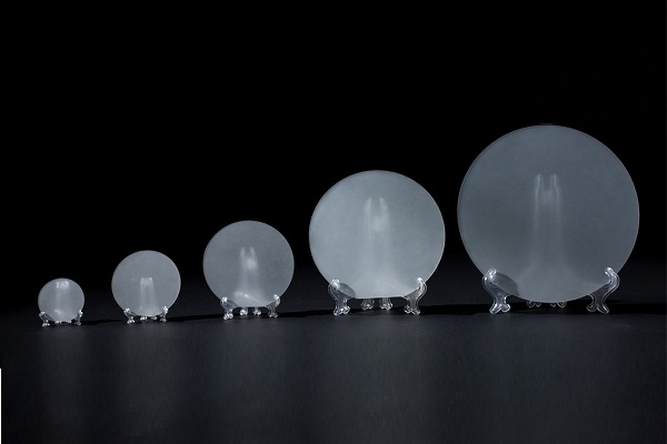
Bulk-GaN Wafers
Bulk-GaN Wafers
Description

Bulk-GaN (Gallium Nitride) wafers are a type of semiconductor material used in the production of high-power electronic and optoelectronic devices. GaN is a wide-bandgap semiconductor material, which means that it has a higher breakdown voltage and can operate at higher temperatures than conventional semiconductors such as silicon.
Bulk-GaN wafers are typically produced using a process called hydride vapor phase epitaxy (HVPE). In this process, a substrate made of sapphire or silicon carbide is heated in the presence of a source material containing gallium and nitrogen. The gallium and nitrogen react to form a thin GaN layer on the substrate. The process is repeated several times to form a thick layer of GaN on the substrate.
Once the GaN layer is grown, it is sliced into thin wafers and polished to a high degree of flatness and smoothness. The resulting Bulk-GaN wafers can then be used as a platform for the growth of additional semiconductor layers, which can be doped with impurities to create p-type and n-type regions for device fabrication.
Bulk-GaN wafers have several advantages over other semiconductor materials such as silicon. GaN has a higher electron mobility and saturation velocity than silicon, which means that it can operate at higher frequencies and with lower power consumption. Additionally, GaN has a wider bandgap than silicon, which makes it suitable for applications such as high-power electronic devices, high-frequency devices, and optoelectronic devices such as LEDs and laser diodes.
| Features | Units | Available planes | |
| C-plane (0001) | |||
| Carrier concentraton | cm-3 | ~1019 | |
| Dopant | Oxygen | ||
| Resistvity | Ωcm | ~10-3 | |
| Mobility | cm2 / Vs | ~150 | |
| Thickness | µm | 350 ±50 | |
| TTV | µm | ≤40 | |
| Bow | µm | ≤10 | |
| FWHM (0002) of XRC,(epi-ready; 0.1x0.1 mm slit) | arcsec | ~20 | |
| Etch Pits Density (EPD) | cm-2 | ~5x10⁴ | |
| Off-cut | deg | 0.3±0.1 to the m-direction | |
| Surface fnishing | Front side | epi-ready (RMS < 0.5 nm) | |
| Back side | rough | ||
| Available sizes | 1-inch | ||
| 2-inch | |||
| Packaging | separate single wafer container | ||
| Special request | for pricing or technical enquiries please contact our sales team | ||
| Features | Units | Available planes | |
| C-plane (0001) | |||
| Carrier concentraton | cm-3 | ~1018 | |
| Dopant | Oxygen | ||
| Resistvity | Ωcm | 10-2 -10-1 | |
| Mobility | cm2 / Vs | ~250 | |
| Thickness | µm | 350 ±50 | |
| TTV | µm | ≤40 | |
| Bow | µm | ≤10 | |
| FWHM (0002) of XRC,(epi-ready; 0.1x0.1 mm slit) | arcsec | ~20 | |
| Etch Pits Density (EPD) | cm-2 | ~5x10⁴ | |
| Off-cut | deg | 0.3±0.1 to the m-direction | |
| Surface fnishing | Front side | epi-ready (RMS < 0.5 nm) | |
| Back side | rough | ||
| Available sizes | 1-inch | ||
| 2-inch | |||
| Packaging | separate single wafer container | ||
| Special request | for pricing or technical enquiries please contact our sales team | ||
| Features | Units | Available planes | |
| C-plane (0001) | |||
| Carrier concentraton | cm-3 | - | |
| Dopant | Manganese-doped (~1019 cm-3) | ||
| Resistvity | Ωcm | >109 | |
| Mobility | cm2 / Vs | - | |
| Thickness | µm | 350 ±50 | |
| TTV | µm | ≤40 | |
| Bow | µm | ≤10 | |
| FWHM (0002) of XRC,(epi-ready; 0.1x0.1 mm slit) | arcsec | ~20 | |
| Etch Pits Density (EPD) | cm-2 | ~5x10⁴ | |
| Off-cut | deg | 0.3±0.1 to the m-direction | |
| Surface fnishing | Front side | epi-ready (RMS < 0.5 nm) | |
| Back side | rough | ||
| Available sizes | 10x10mm | ||
| 1-inch | |||
| 1.5-inch | |||
| Packaging | separate single wafer container | ||
| Special request | for pricing or technical enquiries please contact our sales team | ||
Order Form
About Semiconductor Electronics
SEMI EL project is a global supplier of materials, equipment, spare parts and supplies for the semiconductor industry.
Get In Touch
Email: info@semi-el.com

