Diamond Wafer Heat Sink
Diamond Wafer Heat Sink
Description

Diamond Heat Sink Wafers are a type of semiconductor material used in the production of high-performance electronic devices that require excellent thermal conductivity and heat dissipation. Diamond is the most thermally conductive material known, with a thermal conductivity five times higher than copper and over twenty times higher than silicon. This makes diamond an ideal material for high-power and high-temperature electronic devices.
Diamond heat sink wafers are produced using chemical vapor deposition (CVD) or high-pressure high-temperature (HPHT) techniques. In the CVD method, a gas mixture containing carbon and hydrogen is introduced into a vacuum chamber, where it is heated to high temperatures to break down the gas molecules. The carbon atoms then deposit onto a substrate, forming a diamond film. In the HPHT method, a small diamond seed crystal is placed in a press and subjected to high pressure and high temperature conditions to promote diamond crystal growth.
Once the diamond crystal is grown, it is sliced into thin wafers and polished to a high degree of flatness and smoothness. The resulting diamond heat sink wafers can then be used as a platform for the production of high-performance electronic devices, such as high-power transistors and diodes.
Diamond heat sink wafers offer several advantages over other semiconductor materials such as silicon and aluminum nitride. In addition to high thermal conductivity, diamond also has excellent electrical insulation properties, high mechanical strength, and is resistant to chemical corrosion. This makes diamond heat sink wafers ideal for high-performance electronic devices that require high power operation and high-temperature environments.
We supply thermal grade polycrystalline diamond that can be used as an efficient heat sink to solve the heat dissipation issues in temperature sensitive devices, such as power devices, lasers and photodiodes etc. We also provide wafer form polished diamond substrates with sub-nanometer RMS surface roughness, which is suitable for the integration of GaN, Ga2O3 and AlN epilayers and devices on diamond via direct bonding or epitaxial growth.
Characteristics of CVD Diamond:
✔ Extreme hardness
✔ Ultra high thermal conductivity (1000-2000W/mK,a few times higher than copper)
✔ Wide optical transparency range
✔ Chemical inertness, not affected by acids or other chemicals
✔ Graphitization only at very high temperatures (T>700℃ in with oxygen content and 1500℃ in an inert atmosphere)
We offer Diamond Thermal Management solutions
✔ Thermal conductivity for performance and cost requirements
✔ Custom sizes and shapes for specific applications
✔ Optical transparency any proper applications
✔ Bonding efficacy and layer performance
| Product name | Wafer level diamond (Dia 0.5) | Diamond heat sink (Dia 30) |
| Growth Method | MPCVD | MPCVD |
| Thickness | 0-500 um; customized | 0-500 um; customized |
| Thickness tolerance | ±20 um | ±20 um |
| Size | 2 inch; customized | 2 inch; customized |
| Roughness of growth surface (Ra) | <1nm | <30nm |
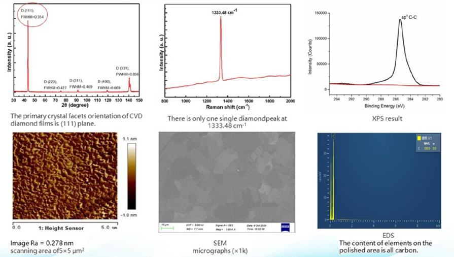
| FWNM (D111) | 0.354 | 0.354 |
| Coefficient of thermal expansion | 1.3(10·6K·1) | 1.3(10·6K·1) |
| Thermal conductivity (T.C) | 1000·2000W/m.K | 1000·2000W/m.K |
| TTV | ≤15μm | ≤15μm |
| Warp | ≤40μm | ≤40μm |
| Bow | ≤30μm | ≤30μm |
Order Form
About Semiconductor Electronics
SEMI EL project is a global supplier of materials, equipment, spare parts and supplies for the semiconductor industry.
Get In Touch
Email: info@semi-el.com