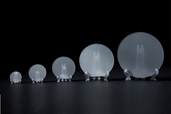
Gallium Arsenide (GaAs) Wafers
Gallium Arsenide (GaAs) Wafers and Substrates
Description

Gallium arsenide (GaAs) wafers and substrates are a type of semiconductor material used in the production of high-speed electronic devices such as field-effect transistors (FETs), power amplifiers, and light-emitting diodes (LEDs). GaAs has a high electron mobility and a direct bandgap, which make it suitable for applications that require high-frequency operation and efficient light emission.
GaAs wafers and substrates are typically produced using the liquid encapsulated Czochralski (LEC) method or the vertical gradient freeze (VGF) method. In the LEC method, a seed crystal is dipped into a molten GaAs solution, which then solidifies into a single crystal as it is slowly pulled out of the solution. The VGF method involves heating a mixture of Ga and As in a furnace, creating a temperature gradient that allows a GaAs crystal to grow from a seed crystal.
Once the GaAs crystal is grown, it is sliced into thin wafers and polished to a high degree of flatness and smoothness. The resulting GaAs wafers and substrates can then be used as a platform for the growth of additional semiconductor layers, which can be doped with impurities to create p-type and n-type regions for device fabrication.
GaAs wafers and substrates have several advantages over other semiconductor materials such as silicon. GaAs has a higher electron mobility than silicon, which means that it can operate at higher frequencies and with lower power consumption. Additionally, GaAs has a direct bandgap, which allows for efficient light emission and makes it suitable for applications such as LEDs and solar cells.
| Item | Unit | LD Applications Specifications | LED Applications | Microelectronics Specifications |
|---|---|---|---|---|
| Conduct Type | n-type | p-type/n-type | ||
| Crystal Growth Method | VGF | VGF | VGF | |
| Dopant | Si | Zn/Si | Undoped | |
| Diameter | inch | 2",3",4" and 6" | 2",3",4" and 6" | 2",3",4" and 6" |
| Wafer Orientation* | (100)±0.1° | (100)±0.5° | (100)±0.5° | |
| OF/IF | US or EJ | US or EJ | US, EJ or notch | |
| Carrier Concentration | /cm3 | (0.4-2.5) ×1018 | (0.5-5) ×1019 (0.4-4)×1018 | |
| Resistivity (at RT) | ohm.cm | (1.2-9.9) ×10-3 | (1.2-9.9)×10-3 | >107 |
| Mobility | cm2/v.s | >1500 | 50-120/>1000 | >4000 |
| Etch Pit Density (EPD) | /cm2 | <500 | <5000 | <5000 |
| Laser Marking | Upon request | Upon request | Upon request | |
| Thickness* | μm | (350-650)±25 | (350-650)±25 | (350-650)±25 |
| TTV(P/P) | μm | ≤5 | ≤5 | ≤4 |
| TTV(P/E) | μm | ≤10 | ≤10 | ≤10 |
| Warp | μm | ≤10 | ≤10 | ≤10 |
| Surface | Side1 Side2 | Polished Polished/Etched | Polished Polished/Etched | Polished Polished/Etched |
| Epi-ready | Yes | Yes | Yes | |
| Package | Cassette or single wafer container | Cassette or single wafer container | Cassette or single wafer container |
Order Form
About Semiconductor Electronics
SEMI EL project is a global supplier of materials, equipment, spare parts and supplies for the semiconductor industry.
Get In Touch
Email: info@semi-el.com

