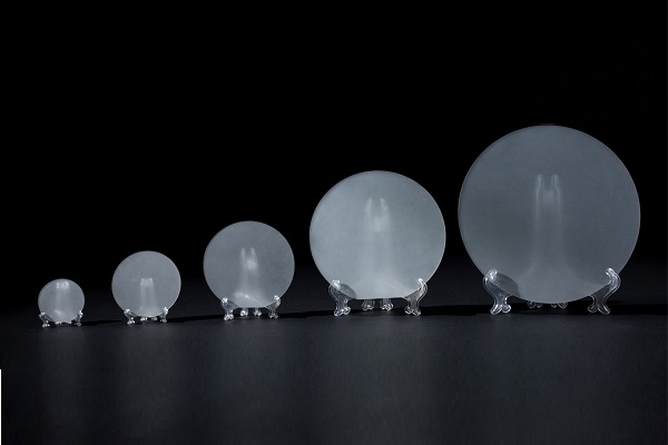
Germanium (Ge) Wafers
Germanium (Ge) Wafers and Substrates
Description

Germanium (Ge) wafers and substrates are a type of semiconductor material used in the production of electronic and optoelectronic devices such as transistors, diodes, and solar cells. Germanium is a Group IV element and has a crystalline structure similar to silicon, but with some important differences in its physical properties.
Germanium wafers and substrates are typically produced using the Czochralski (CZ) method, where a seed crystal is dipped into a melt of molten germanium and slowly pulled out while rotating. The molten germanium solidifies and forms a single crystal as the seed crystal is pulled out.
Once the germanium crystal is grown, it is sliced into thin wafers and polished to a high degree of flatness and smoothness. The resulting germanium wafers and substrates can then be used as a platform for the growth of additional semiconductor layers, which can be doped with impurities to create p-type and n-type regions for device fabrication.
Germanium wafers and substrates have several advantages over other semiconductor materials such as silicon. Germanium has a higher electron mobility than silicon, which means that it can operate at higher frequencies and with lower power consumption. Additionally, germanium has a narrower bandgap than silicon, which makes it suitable for applications such as near-infrared photodetectors and solar cells.
Overall, germanium wafers and substrates are an important semiconductor material for a wide range of electronic and optoelectronic applications, particularly those requiring high-speed performance in the near-infrared wavelength range.
Ge wafers are offer in sizes 2 inch and 4 inch and are used in microelectrinics, optoelectrincs, optics. Ge wafers are used to manufacture solar cells for space and terrestrial applications, optical lens, light emitting diodes (LED) and photodetectors.
| Item | Unit | Semiconduct Specifications | |
|---|---|---|---|
| Crystal Growth Method | CZ | ||
| Conduct Type | (n-type) | (p-type) | |
| Dopant | As,Sb | Ga | |
| Diameter | inch | 2",3",4" and 6" | |
| Wafer Orientation | (100)±0.5° | ||
| OF/IF | US,EJ | ||
| Laser Marking | /cm3 | Upon request | |
| Thickness | μm | (175-500)±25 | |
| Resistivity (at RT) | ohm.cm | 0.005-30 | 0.005-0.04 |
| Etch Pit Density (EPD) | /cm2 | - | 0 |
| TTV | μm | ≤15 | ≤15 |
| Warp | μm | ≤25 | ≤25 |
| Backside Ra | μm | <0.1 | <0.1 |
| Surface | Side1/Side2 | E/E, P/E, P/D | |
| Epi-ready | Yes | ||
| Package | Cassette or single wafer container | ||
Order Form
About Semiconductor Electronics
SEMI EL project is a global supplier of materials, equipment, spare parts and supplies for the semiconductor industry.
Get In Touch
Email: info@semi-el.com

