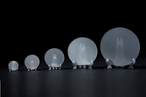
Indium Antimonide InSb Wafers
Indium Antimonide InSb Wafers
Description

Indium Antimonide (InSb) wafers are a type of semiconductor material used in the production of electronic and optoelectronic devices that operate in the mid-infrared range. InSb is a narrow-bandgap semiconductor material, which means that it has a smaller bandgap than conventional semiconductors such as silicon.
InSb wafers are typically produced using the liquid phase epitaxy (LPE) or molecular beam epitaxy (MBE) methods. In the LPE method, a substrate made of InSb is immersed in a molten solution containing indium and antimony. The substrate is then slowly pulled out of the solution, allowing a single crystal InSb layer to grow on the substrate. In the MBE method, a substrate made of InSb is heated in a vacuum chamber and a source material, typically indium and antimony, is heated until it vaporizes. The vapor is transported by a carrier gas, typically hydrogen, and deposited on the InSb substrate, forming a single crystal InSb layer.
Once the InSb crystal is grown, it is sliced into thin wafers and polished to a high degree of flatness and smoothness. The resulting InSb wafers can then be used as a platform for the growth of additional semiconductor layers, which can be doped with impurities to create p-type and n-type regions for device fabrication.
InSb wafers have several advantages over other semiconductor materials such as silicon. InSb has a high electron mobility and a high electron saturation velocity, which makes it suitable for high-speed electronic devices. Additionally, InSb has a large absorption coefficient in the mid-infrared range, which makes it suitable for applications such as infrared detectors and imaging systems.
| Items | Standard Specification | ||
| Size | 2" | 3" | 4" |
| Diameter mm | 50.5±0.5 | 76.2±0.5 | 100±0.5 |
| Growth Method | LEC | LEC | LEC |
| Conductivity | P/(Zn-doped or un-doped), N/Te-doped | ||
| Orientation | (100)±0.5°, (111)±0.5° | ||
| Thickness μm | 500±25 | 600±25 | 800±25 |
| Orientation Flat mm | 16±2 | 22±1 | 32.5±1 |
| Identification Flat mm | 8±1 | 11±1 | 18±1 |
| Mobility cm2/V.s | 200-3500 or as required | ||
| Carrier Concentration cm-3 | (1-100)E17 or as required | ||
| TTV μm max | 15 | 15 | 15 |
| Bow μm max | 15 | 15 | 15 |
| Warp μm max | 20 | 20 | 20 |
| Dislocation Density cm-2 max | 500 | 1000 | 2000 |
| Surface Finish | P/E, P/P | P/E, P/P | P/E, P/P |
| Packing | Single wafer container sealed in Aluminum bag. | ||
Order Form
About Semiconductor Electronics
SEMI EL project is a global supplier of materials, equipment, spare parts and supplies for the semiconductor industry.
Get In Touch
Email: info@semi-el.com

