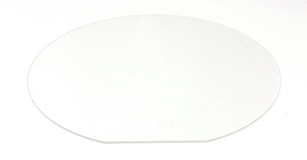
Optical grade LiNbO3 wafers SLN CLN
Optical grade LiNbO3 wafers SLN CLN
Description

Lithium Niobate has good electro-optic and acousto-optic characteristics. Due to these properties LN wafers are used in optical applications for electro-optic waveguide amplitude modulation, phase modulators, quasi-phase matching for SHG and OPO, polarizer for optical isolators.
Optical grade lithium niobate (LiNbO3) wafers can be classified into different types based on their dopant concentration and composition. Two common types are SLN (stoichiometric lithium niobate) and CLN (congruent lithium niobate).
SLN wafers are made from a stoichiometric ratio of lithium niobate, which means that the amount of lithium and niobium is balanced. This results in a crystal with a high level of purity and uniformity, making it ideal for use in high-end optical devices, such as waveguides and modulators. SLN wafers have a low coercive field, high optical damage threshold, and high nonlinear coefficient, making them an excellent choice for applications where high optical power is involved.
CLN wafers, on the other hand, are made from a lithium niobate crystal with a slightly higher concentration of niobium. This makes them easier to produce and less expensive than SLN wafers. CLN wafers have a higher coercive field, which means that they are less susceptible to polarization reversal due to external electrical fields. However, they have a lower optical damage threshold and a lower nonlinear coefficient compared to SLN wafers.
Both SLN and CLN wafers are used in a variety of optical applications, such as frequency converters, modulators, and sensors. The choice of wafer type depends on the specific requirements of the application, such as the desired optical properties, electrical properties, and cost.
| Material | Optical Grade LiNbO3 wafes (White or Black) | |
| Curie Temp | 1142±0.7℃ | |
| Cutting Angle | X/Y/Z etc | |
| Diameter/size | 2”/3”/4” ±0.03mm | |
| Tol(±) | <0.20 mm ±0.005mm | |
| Thickness | 0.18 ~ 0.5mm or more | |
| Primary Flat | 16mm/22mm /32mm | |
| TTV | <3µm | |
| Bow | -30<bow<30 | |
| Warp | <40µm | |
| Orientation Flat | All available | |
| Surface Type | Single Side Polished(SSP) /Double Sides Polished(DSP) | |
| Polished side Ra | <0.5nm | |
| S/D | 20/10 | |
| Edge Criteria | R=0.2mm C-type or Bullnose | |
| Quality | Free of crack (bubbles and inclusions) | |
| Optical doped | Mg/Fe/Zn/MgO etc for optical grade LN< wafers per requested | |
| Wafer Surface Criteria | Refractive index | No=2.2878/Ne=2.2033 @632nm wavelength/prism coupler method. |
| Contamination, | None | |
| Particles ¢>0.3 µ m | <= 30 | |
| Scratch , Chipping | None | |
| Defect | No edge cracks, scratches, saw marks, stains | |
| Packaging | Qty/Wafer box | 25pcs per box |
Order Form
About Semiconductor Electronics
SEMI EL project is a global supplier of materials, equipment, spare parts and supplies for the semiconductor industry.
Get In Touch
Email: info@semi-el.com

