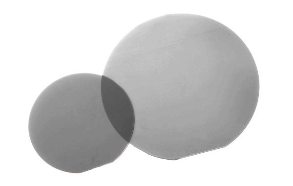
SAW Grade LiNbO3 (Black) Wafer
SAW Grade LiNbO3 (Black) Wafer
Description

Black Lithium Niobate has the same piezoelectric properties as regular LN and is used in SAW device manufacturing. The difference of black LN is that it has lower pyroelectric charges due to higher electrical conductivity and high near UV absorption.
SAW (Surface Acoustic Wave) grade lithium niobate wafers are a special type of lithium niobate wafer that is used for surface acoustic wave devices. These devices are used in a variety of applications, such as wireless communications, radar systems, and sensors.
The process of producing SAW grade lithium niobate wafers involves growing a high-purity lithium niobate crystal using advanced crystal growth techniques, such as the Czochralski method or the Bridgman-Stockbarger technique. The resulting crystal is then sliced into wafers and polished to a high degree of flatness and smoothness.
SAW grade lithium niobate wafers are characterized by their high piezoelectric coefficient and low insertion loss. These properties make them ideal for use in surface acoustic wave devices, where they can efficiently convert electrical signals into acoustic waves and vice versa.
Surface acoustic wave devices that use SAW grade lithium niobate wafers include resonators, filters, and delay lines. These devices are important components in many electronic systems and are used to filter out unwanted signals, amplify signals, and delay signals in time.
| Material | LiNbO3 wafers (White or Black) | |
| Curie Temp | 1142±2.0℃ | |
| Cutting Angle | X/Y/Z/Y36/Y41/Y64/Y128/etc | |
| Diameter/size | 3”/4”/6"LN wafer & 8"under R/D | |
| Tol(±) | <0.20 mm | |
| Thickness | 0.18 ~ 0.5mm or more | |
| Primary Flat | 22mm /32mm /42.5mm /57.5mm | |
| LTV (5mmx5mm) | <1µm | |
| TTV | <3µm | |
| Bow | -30<bow<30 | |
| Warp | <40µm | |
| PLTV(<0.5um) | ≥95%(5mm*5mm) | |
| Orientation Flat | All available | |
| Surface Type | Single Side Polished /Double Sides Polished | |
| Polished side Ra | <0.5nm | |
| Back Side Criteria | General is 0.2-0.5µm or as customized | |
| Edge Criteria | R=0.2mm or Bullnose | |
| Wafer Surface Criteria | Transmissivity | general:5.9x10⁻¹¹<s<2.0*10-10 at 25℃ |
| Contamination, | None | |
| Particles ¢>0.3 µ m | <= 30 | |
| Scratch , Chipping | None | |
| Defect | No edge cracks, scratches, saw marks, stains | |
| Packaging | Qty/Wafer box | 25pcs per box |
Order Form
About Semiconductor Electronics
SEMI EL project is a global supplier of materials, equipment, spare parts and supplies for the semiconductor industry.
Get In Touch
Email: info@semi-el.com

