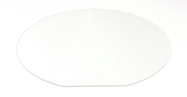
Fe Doped LiTaO3 Wafer
Fe Doped LiTaO3 Wafer
Description

Fe-doped Lithium Tantalate (LiTaO3) wafers are a special type of lithium tantalate wafer that is doped with iron (Fe) ions. The doping process involves adding small amounts of iron to the melt during the crystal growth process, resulting in a crystal with a controlled concentration of Fe ions.
Fe-doped LiTaO3 wafers are used in a variety of applications, including electro-optic and magneto-optic devices. The presence of Fe ions in the crystal lattice of LiTaO3 results in a magneto-optic effect, which allows for the manipulation of the polarization of light using an external magnetic field.
The magneto-optic effect of Fe-doped LiTaO3 wafers makes them ideal for use in magnetic field sensors, modulators, and isolators. They are also used in telecommunications, where they are used to convert optical signals into electrical signals and vice versa.
Fe-doped LiTaO3 wafers have other unique properties that make them useful in a variety of applications. For example, they have a high Curie temperature, which means that they can operate at high temperatures without losing their ferroelectric properties. They also have a high electro-optic coefficient, which makes them useful in electro-optic devices.
| Material | LiTaO3 wafers(White or Black &Fe doped) | |
| Curie Temp | 603±2℃ | |
| Cutting Angle | X/Y/Z/X112Y/Y36/Y42/Y48/etc | |
| Diameter/size | 3”/4”/6" LT wafer | |
| Tol(±) | <0.20> | |
| Thickness | 0.18 ~ 0.5mm or more | |
| Primary Flat | 22mm /32mm /42.5mm /57.5mm | |
| LTV (5mmx5mm) | <1µm | |
| TTV | <3µm | |
| Bow | -30 | |
| Warp | <40µm | |
| PLTV( <0.5um) | ≥95%(5mm*5mm) | |
| Orientation Flat | All available | |
| Surface Type | Single Side Polished /Double Sides Polished | |
| Polished side Ra | <0.5nm | |
| Back Side Criteria | General is 0.2-0.5µm or as customized | |
| Edge Criteria | R=0.2mm or Bullnose | |
| Fe doped | Fe doped for saw grade LN <> | |
| Wafer Surface Criteria | Transmissivity | general:5.9x10⁻¹¹<s<2.0*10-10 at 25℃ |
| Contamination, | None | |
| Particles ¢>0.3 µ m | <=> | |
| Scratch , Chipping | None | |
| Defect | No edge cracks, scratches, saw marks, stains | |
| Packaging | Qty/Wafer box | 25pcs per box |
Order Form
About Semiconductor Electronics
SEMI EL project is a global supplier of materials, equipment, spare parts and supplies for the semiconductor industry.
Get In Touch
Email: info@semi-el.com

