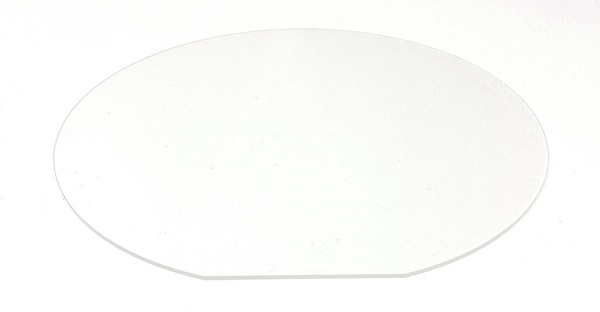
SAW Grade LiTaO3 Wafer
SAW Grade LiTaO3 Wafer
Description

LiTaO3 wafers have the properties that allow to use them in a number of applications for SAW and BAW devices. Wafers can have different properties like optical, SAW grade and pyroelectric discharge free or black LN wafers.the 36 and 42-cut LT wafers are widely used in devices for telecom and mobile applications for frequency range 800 to 2200MHz.
SAW (Surface Acoustic Wave) grade Lithium Tantalate (LiTaO3) wafers are a type of single-crystal wafer that is specifically designed for use in surface acoustic wave devices. These wafers are carefully grown and processed to have precise characteristics that are important for achieving optimal SAW device performance.
SAW grade LiTaO3 wafers are typically grown using the Czochralski method, which involves melting a high-purity LiTaO3 crystal and slowly pulling it from the melt to form a single-crystal ingot. The ingot is then sliced into thin wafers, which are polished to a high degree of flatness and surface quality.
The properties of SAW grade LiTaO3 wafers make them ideal for use in SAW devices, which are used in a variety of applications, including telecommunications, sensing, and navigation systems. SAW devices are based on the piezoelectric properties of the crystal, which allows for the conversion of electrical signals into acoustic waves that travel along the surface of the crystal.
SAW grade LiTaO3 wafers have specific characteristics that are optimized for SAW device performance, such as a high electromechanical coupling coefficient and a low temperature coefficient of delay. These properties are critical for achieving high-frequency operation and stable performance over a wide temperature range.
| Material | LiTaO3 wafers(White or Black) | |
| Curie Temp | 603±2℃ | |
| Cutting Angle | X/Y/Z/X112Y/Y36/Y42/Y48/etc | |
| Diameter/size | 3”/4”/6" LT wafer | |
| Tol(±) | <0.20 mm="" td=""> | |
| Thickness | 0.18 ~ 0.5mm or more | |
| Primary Flat | 22mm /32mm /42.5mm /57.5mm | |
| LTV (5mmx5mm) | <1µm | |
| TTV | <3µm | |
| Bow | -30<bow<30 | |
| Warp | <40µm | |
| PLTV(<0.5um) | ≥95%(5mm*5mm) | |
| Orientation Flat | All available | |
| Surface Type | Single Side Polished /Double Sides Polished | |
| Polished side Ra | <0.5nm | |
| Back Side Criteria | General is 0.2-0.5µm or as customized | |
| Edge Criteria | R=0.2mm or Bullnose | |
| Wafer Surface Criteria | Transmissivity | general:5.9x10⁻¹¹<s<2.0*10-10 at 25℃ |
| Contamination, | None | |
| Particles ¢>0.3 µ m | <= 30 | |
| Scratch , Chipping | None | |
| Defect | No edge cracks, scratches, saw marks, stains | |
| Packaging | Qty/Wafer box | 25pcs per box |
Order Form
About Semiconductor Electronics
SEMI EL project is a global supplier of materials, equipment, spare parts and supplies for the semiconductor industry.
Get In Touch
Email: info@semi-el.com

