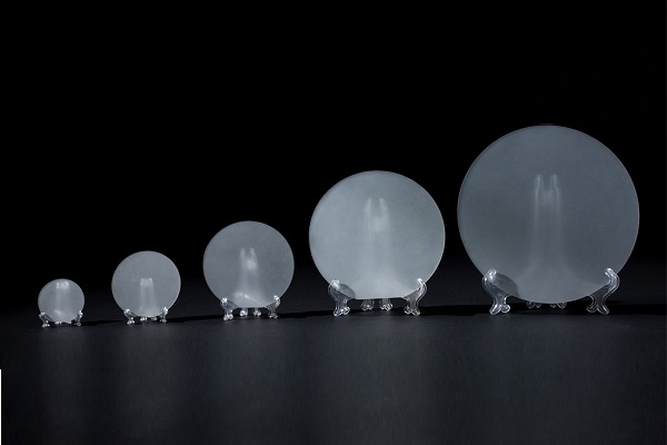
Silicon Carbide (SiC) Wafers
Silicon Carbide (SiC) Wafers
Description

Silicon Carbide (SiC) wafers are a type of semiconductor material used in the production of electronic and optoelectronic devices that require high-temperature, high-voltage, and high-frequency operation. SiC is a wide-bandgap semiconductor material, which means that it has a higher breakdown voltage and can operate at higher temperatures than conventional semiconductors such as silicon.
SiC wafers are typically produced using the physical vapor transport (PVT) or chemical vapor deposition (CVD) methods. In the PVT method, a seed crystal of SiC is placed in a high-temperature furnace and a source material, typically silicon or carbon, is heated until it vaporizes. The vapor is transported by a carrier gas, typically argon, and deposited on the seed crystal, forming a single crystal SiC layer. In the CVD method, a SiC layer is deposited on a substrate by reacting a gas mixture containing silicon and carbon precursors at high temperatures.
Once the SiC crystal is grown, it is sliced into thin wafers and polished to a high degree of flatness and smoothness. The resulting SiC wafers can then be used as a platform for the growth of additional semiconductor layers, which can be doped with impurities to create p-type and n-type regions for device fabrication.
SiC wafers have several advantages over other semiconductor materials such as silicon. SiC has a higher thermal conductivity, which means that it can operate at higher temperatures without suffering from thermal breakdown. Additionally, SiC has a higher breakdown voltage and can operate at higher voltages and frequencies than silicon, making it suitable for applications such as high-power electronics and high-frequency devices.
| Growth Method | Physical Vapor Transport | |
| Physical Properties | ||
| Structure | Hexagonal, Single Crystal | |
| Diameter | Up to 150mm, 200mm | |
| Thickness | 350µm (n-type, 3″ SI), 500µm (SI) | |
| Grades | Prime, Development, Mechanical | |
| Thermal Properties | ||
| Thermal Conductivity | 370 (W/mK) at Room Temperature | |
| Thermal Expansion Coefficient | 4.5 (10-6K-1) | |
| Specific Heat (25⁰C) | 0.71 (J g-1 K-1) | |
| Additional Key Properties of II-VI SiC Substrates (typical values*) | ||
| Parameter | N-type | Semi-insulating |
| Polytype | 4H | 4H, 6H |
| Dopant | Nitrogen | Vanadium |
| Resistivity | ~0.02 Ohm-cm | > 1∙1011 Ohm-cm |
| Orientation | 4° off-axis | On-axis |
| FWHM | < 20 arc-sec | < 25 arc-sec |
| Roughness, Ra** | < 5 Å | < 5 Å |
| Dislocation density | ~5∙103 cm-2 | < 1∙104 cm-2 |
| Micropipe density | < 0.1 cm-2 | < 0.1 cm-2 |
| Growth Method | Physical Vapor Transport | |
| Physical Properties | ||
| Structure | Hexagonal, Single Crystal | |
| Diameter | Up to 150mm, 200mm | |
| Thickness | 350µm (n-type, 3″ SI), 500µm (SI) | |
| Grades | Prime, Development, Mechanical | |
| Thermal Properties | ||
| Thermal Conductivity | 370 (W/mK) at Room Temperature | |
| Thermal Expansion Coefficient | 4.5 (10-6K-1) | |
| Specific Heat (25⁰C) | 0.71 (J g-1 K-1) | |
| Additional Key Properties of II-VI Materials SiC Substrates (typical values*) | ||
| Parameter | N-type | Semi-insulating |
| Polytype | 4H | 4H, 6H |
| Dopant | Nitrogen | Vanadium |
| Resistivity | ~0.02 Ohm-cm | > 1∙1011 Ohm-cm |
| Orientation | 4° off-axis | On-axis |
| FWHM | < 20 arc-sec | < 25 arc-sec |
| Roughness, Ra** | < 5 Å | < 5 Å |
| Dislocation density | ~5∙103 cm-2 | < 1∙104 cm-2 |
| Micropipe density | < 0.1 cm-2 | < 0.1 cm-2 |
Order Form
About Semiconductor Electronics
SEMI EL project is a global supplier of materials, equipment, spare parts and supplies for the semiconductor industry.
Get In Touch
Email: info@semi-el.com

